
imec Says Fabs Can't Measure Every Wafer. So 95% Are Predicted.
Only 1–5% of Wafers Get Measured. A Model Writes the Rest.
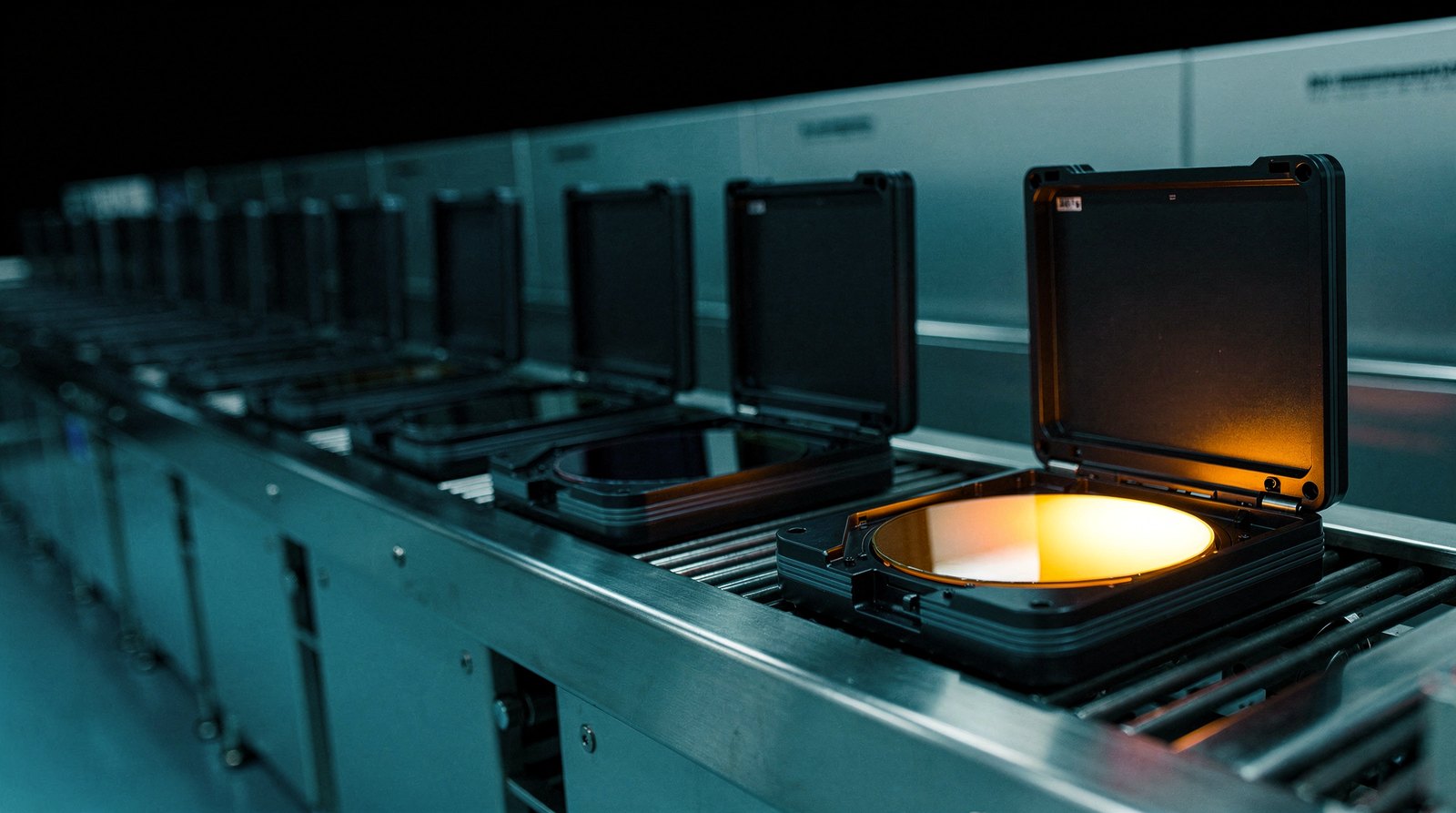
This one has not been published to the channel yet. Subscribe on YouTube and it will turn up there.
PHYSICAL VALIDATION
- Why not just measure them all?
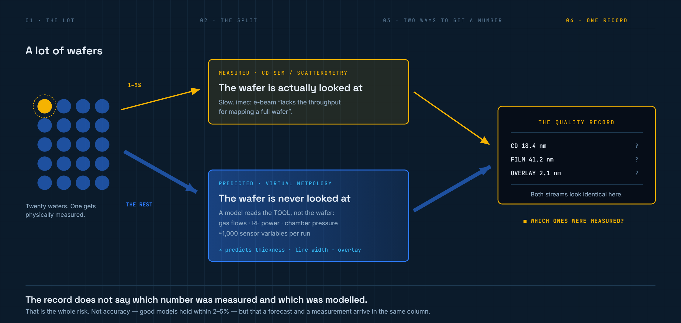
- As imec put it in July 2026, e-beam inspection "lacks the throughput for mapping a full wafer" — check every one and you stop the line.
- And the models are good: two to five percent error on stable processes, with fabs reporting ten to twenty percent more throughput for it.
- Most of it is now a forecast, sitting in the same column, in the same font, as the measurements — with nothing on the row to tell you which is which.
Why this matters
In a fab running virtual metrology, only one to five percent of wafers are physically measured. The rest get a number anyway — predicted by a model that reads the process tools rather than the wafer: gas flows, RF power, chamber pressure, roughly a thousand sensor variables per run, turned into a thickness, a line width, an overlay. So this is not a story about AI being wrong. It's about what your quality record now IS.
It used to be evidence that something was inspected.
The same idea, pointed at your AI. Paste this under any question that matters: "Before you answer, label every factual claim [VERIFIED] / [INFERRED] / [UNKNOWN]. VERIFIED = you could name where it comes from. INFERRED = you're reasoning from patterns, not a fact you hold. Then give me a SAMPLING RATE: what fraction of your claims are VERIFIED?" I ran this on a chip-industry question this week. It refused to give me a 2026 capital-spending figure, labelled it UNKNOWN, and said that without the labels it would have produced one — and that it would have looked right. It does NOT make the answer more accurate; it stops the unverified lines looking identical to the verified ones. You already do this in a spreadsheet — which cells were typed, which were calculated. Two honest limits: it's self-report, not verification, so treat it as a triage list; and the labels drift in long conversations, so re-issue it on anything that matters.
Do you know which numbers in your quality system were measured, and which were modelled? And could you find out today if someone asked?
Argue with me on LinkedIn- imec — "Four decades of in-fab metrology and inspection: pivotal milestones and the road ahead", 27 July 2026, by Anne-Laure Charley (R&D Metrology Manager) and Philippe Leray (VP R&D Advanced Patterning Development). Source of the quoted line that e-beam inspection "lacks the throughput for mapping a full wafer", and of the description of virtual metrology as physical-tool data "complemented and extended with data coming from a virtual metrology model". imec's stated road ahead is BOTH better hardware (multi-head AFM, multi-beam e-beam) AND more algorithmic deployment — they do not present prediction as a replacement for measurement, and this video does not claim they do.
- Virtual-metrology practitioner guidance (April 2026) — the operating numbers: 100–1,000 process variables per run (optical emission spectroscopy, voltage/current waveforms, mass-flow-controller data, RF power profiles, gas analyser outputs); residual physical validation of 1–5% of wafers described as "non-negotiable" after deployment; mean absolute percentage error of 2–5% on stable, well-modelled processes with R² above 0.95; 10–20% throughput uplift and 20–50% metrology cost saving over 6–12 months. ⚠ These are PRACTITIONER- AND VENDOR-REPORTED RANGES, not audited results, and they describe fabs that have ALREADY deployed virtual metrology — the 1–5% figure is NOT the industry-wide sampling rate today. The video says "in a fab running virtual metrology" for that reason.
- Industry position that at sub-3nm nodes with AI-chip volumes, predicting critical dimension, film thickness and overlay from sensor data is the only economically viable route to wafer-level quality control.
- HACK OF THE WEEK: executed first-hand for this video, not quoted from documentation. The full transcript of what the model returned, including its own account of what the labels changed, is in the run's tip-validation file. No vendor endorsed. imec is named because it is the source of the quoted claim. Nothing here characterises any company or technology negatively — the video states plainly that the models are accurate and that fabs report real throughput gains.
Full transcript, 284 spoken words
Keep reading
All pieces
AI Now Lets Chip Fabs "Measure" Wafers They Never Touch (Virtual Metrology)
Chip factories physically measure only about 3 wafers in 100. For the other 97, an AI called virtual metrology predicts the exact dimension straight from the process tool's own sensor "fingerprint" — pressure, power, gas flow, hundreds of signals per wafer — in milliseconds, with no measurement step and no throughput hit.
Your Fab's AI Goes Blind on the 2nm Node — Here's Why
Your fab's new AI spots defects better than any engineer — and on the brand-new node it goes almost blind. Not because the model is bad, but because every one of these systems learns from history: thousands of wafers, labelled defects, known-good outcomes.
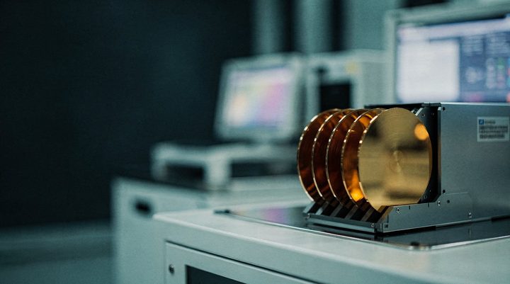
Chip Factories Only Check 10% of Their Wafers — Here's the AI That Sees the Rest
A modern chip fab physically measures fewer than 1 in 10 wafers — the other 90% ship out never directly checked, because real metrology is slow and a fab runs thousands of wafers a day. In 2026 that changed: AI "virtual metrology" now predicts the quality of the wafers you never measured, straight from the…